Physical Layer Clock Protection Switching
This section describes how to deploy a highly reliable clock synchronization network and covers the following topics:
Overview of Clock Protection Switching
Implementation of Clock Protection Switching
Boards Participating in Clock Protection Switching
Overview of Physical Layer Clock Protection Switching
Each router traces the same reference clock level by level over clock synchronization paths to implement clock synchronization on the entire network. Usually, a router may have many clock sources, which may come from either the same master clock or from reference clocks with different qualities. Maintaining synchronous router clocks is very important on a synchronization network. Automatic protection switching of synchronized clocks can be configured to prevent the entire synchronization network from becoming faulty because of a faulty clock synchronization path.
Automatic protection switching of synchronized clocks means that when a certain clock source traced by a router is lost, the router automatically traces another clock source, which may be either the same reference clock as the previously traced one or another one of poorer quality. After the previously traced clock source recovers, the router traces the clock source again.
Implementation of Physical Layer Clock Protection Switching
The methods of implementing clock protection switching are as follows:
Specifying a clock source manually
You can configure a clock board to always trace a certain clock source. You can also configure different clock sources for the active and standby clock boards.
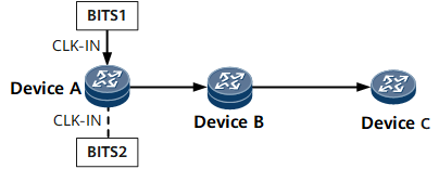
As shown in Figure 1, on Device A that serves as the master clock, the active clock board is configured to trace BITS1 and the standby clock board is configured to trace BITS2. Normally, the master clock traces BITS1. When the active clock board is faulty, an active/standby clock board switchover is implemented. After that, Device A traces BITS2. Device B is configured to trace the clock of Device A, and Device C is configured to trace the clock of Device B.
When all devices on the entire network trace router A's clock, there is no reference clock on the entire network if router A fails. As a result, all routers do not have an accurate reference clock. The routers may trace a reference clock, but the reference clock accuracy cannot meet synchronization requirements.
Performing protection switching based on the priorities of clock sources
When there are multiple reference clock sources, you can set different priorities for them. During protection switching, if the SSM level is configured not to participate in reference source selection, the clock board prefers the reference clock source with the highest priority. After the reference clock source with the highest priority becomes faulty, the clock board selects the reference clock source with the second highest priority. If the default priority (0) of the reference source is used, this reference source is not chosen during protection switching.
Performing protection switching based on SSM levels
An SSM is a group of codes used to indicate the level of the clock quality on a synchronization network. ITU-T dictates that four bits are used for coding. Table 1 lists the SSM codes defined by ITU-T. These four bits comprise the Synchronous Status Message Byte (SSMB). The codes represent 16 quality levels of synchronization sources. When the SSMB of a clock source is 2, the quality of the clock source is of the highest level. When the SSMB of a clock source is f, the quality of the clock source is of the lowest level.
On an SDH transmission network, the SSM is transmitted through the four low-order bits b5 through b8 in the S1 byte of the SDH segment overhead. On a BITS device, however, the SSM is transmitted through a certain bit in the first timeslot (TS0) of the clock signal of 2 Mbit/s. Therefore, 2 MHz clock signals cannot carry the SSM.
The difference between the SSMB and S1 byte is that the SSMB is a group of message codes, representing clock quality levels, as listed in Table 1, whereas the S1 byte is a byte in the SDH segment overhead with the four low-order bits representing the SSMB.
Table 1 SSM codes Z1 (b5-b8)
S1 Byte
SDH Synchronization Quality Level
0000
0x00
Unknown
0001
0x01
Reserved
0010
0x02
G.811 clock signals (PRC, a caesium clock)
0011
0x03
Reserved
0100
0x04
G.812 transit site clock signals (SSUA, a rubidium clock)
0101
0x05
Reserved
0110
0x06
Reserved
0111
0x07
Reserved
1000
0x08
G.812 local site clock signals (SSUB, a rubidium clock or a crystal clock)
1001
0x09
Reserved
1010
0x0a
Reserved
1011
0x0b
SEC (a crystal clock)
1100
0x0c
Reserved
1101
0x0d
Reserved
1110
0x0e
Reserved
1111
0x0f
Cannot be used as a clock source (DNU)
When the clock board is powered on, the default SSM levels of all reference sources are Unknown. The sequence of the SSM levels from high to low is PRC, SSUA, SSUB, SEC, UNKNOWN, and DNU. If the SSM level of a clock source is DNU and the SSM level participates in the selection of a clock source, the clock source is not selected during protection switching.
The SSM level of output signals is determined by the traced clock source. When the clock works in the trace state, the SSM level of output signals and that of the traced clock source are the same. When the clock does not work in the trace state, the SSM level of output signals is SEC.
For a line clock source, the SSM can be extracted from an interface board and reported to the IPU. The IPU then sends the SSM to the clock board. The IPU can also forcibly set the SSM of the line clock source.
For the BITS clock source of the clock module:- If the signal is 2.048 Mbit/s, the clock module can extract the SSM from the signal.
- If the signal is 2.048 MHz, the SSM level can be set manually.

The router can only select an SSM value listed in Table 1. For values not listed, the router processes them as DNU.
Boards Participating in Physical Layer Clock Protection Switching
Clock protection switching involves boards and protocols. The functions of the boards during clock protection switching are as follows:
Interface board
An interface board is responsible for inserting and extracting the SSM. The SSM of the best clock source sent by the clock board is set on each synchronous physical interface on the interface board for distribution. The SSM of the best clock source received by each synchronous interface is processed by the interface board.
Clock board
A clock board extracts the SSMs of an external clock and implements protection switching between clock sources. After receiving SSMs from an interface board, the clock board determines the clock source to be traced based on SSM levels, implements clock protection switching, and sends the SSM level of the current clock source to other interface boards.